Researchers in China and the US have created a functional semiconductor made from graphene, a feat that they describe as a first. By expanding on existing fabrication techniques, Walter de Heer and colleagues at Tianjin University and the Georgia Institute of Technology have created a develop a bandgap in the 2D material, while retaining graphene’s robust and easily tuneable properties.
Silicon is the backbone of modern semiconductor electronics. However, the latest silicon-based technologies are being stretched to their limits by our relentless demand for higher computing speeds, lower power consumption, and more compact devices.
For two decades now, researchers have explored the possibility that graphene could provide a practical alternative to silicon. First isolated in 2004, graphene is a sheet of carbon just one atom thick. Since then, researchers have found that graphene has a number of properties that could make it very useful for electronic devices. These include high electron mobility; a strong, lightweight, highly compact structure; and excellent heat dissipation.
One major drawback
However, graphene has one major drawback. Unlike conventional semiconductors, graphene lacks an intrinsic electron bandgap. This is an energy barrier that electrons must overcome to conduct electricity. It is the bandgap that allows electronic switches (transistors) to be made from semiconductors.
“A long-standing problem in graphene electronics is that graphene didn’t have the right bandgap, and couldn’t switch on and off at the correct ratio,” explains co-author Lei Ma, who co-founded the Tianjin International Center for Nanoparticles and Nanosystems with de Heer. “Over the years, many have tried to address this with a variety of methods.”
Previous studies have tried to engineer appropriate bandgaps using techniques such as quantum confinement and the chemical modification of pure graphene. So far, however, these approaches have resulted in very little success.
“We had to learn how to treat [graphene], how to make it better and better, and finally how to measure its properties,” de Heer explains. “That took a very, very long time.”
Spontaneous growth
In their latest research, the researchers have shown for the first time how the bandgap semiconductor “epigraphene” can been grow spontaneously on the surfaces of silicon carbide crystals.
Previous research had revealed that at high temperatures, silicon sublimates from the surfaces of these crystals, leaving behind carbon-rich layers. These layers recrystallise into multi-layered epigraphene, which has limited semiconducting properties.
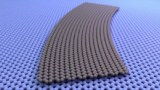
Expanding on this technique, de Heer and Ma’s team have developed a new annealing method, in which they carefully controlled the sample temperature and the rate of epigraphene formation. They created a robust graphene layer that grows in macroscopic, atomically-flat terraces. What is more, the graphene atoms are aligned with the lattice of the silicon carbide substrate.
Useful bandgap
By making careful measurements, the team showed that this layer is an excellent 2D semiconductor. It has the useful bandgap that has eluded researchers for decades, along with high electron mobility.
Graphene ribbons advance twistronics
“We now have an extremely robust graphene semiconductor with 10 times the mobility of silicon, and which also has unique properties not available in silicon,” de Heer enthuses. He compares electron mobility in silicon to driving on a gravel road, whereas the epigraphene is like an electron freeway. “It’s more efficient, it doesn’t heat up as much, and it allows for higher speeds so that the electrons can move faster,” explains de Heer.
On top of this performance, the team also showed that their epigraphene can be doped with a wide range of atoms and molecules to fine-tune its electronic and magnetic properties. The material can also be nanopatterned to further enhance its performance further – nanopatterning is very difficult to do with graphene grown on other substrates.
De Heer, Ma and their colleagues hope that their technique could pave the way for an entirely new approach to semiconductor manufacturing, and may ultimately be a crucial first step towards a new generation of graphene-based electronics.
The research is described in Nature.
- SEO Powered Content & PR Distribution. Get Amplified Today.
- PlatoData.Network Vertical Generative Ai. Empower Yourself. Access Here.
- PlatoAiStream. Web3 Intelligence. Knowledge Amplified. Access Here.
- PlatoESG. Carbon, CleanTech, Energy, Environment, Solar, Waste Management. Access Here.
- PlatoHealth. Biotech and Clinical Trials Intelligence. Access Here.
- Source: https://physicsworld.com/a/graphene-based-semiconductor-has-a-useful-bandgap-and-high-electron-mobility/