A new type of sticky tape that is sensitive to ultraviolet light makes it easier and cheaper to transfer two-dimensional materials like graphene onto different surfaces. According to its Japan-based developers, the new tape technique could revolutionize 2D materials transfer, bringing us closer to integrating such materials into devices.
2D materials form the basis of many advanced electronic and optoelectronics devices. Because they are just a few atoms thick, however, these materials are difficult to transfer onto device surfaces. Current methods are highly complex and often involve etching a substrate with corrosive acids. The materials’ extreme thinness also means they often need a polymer film to support them during the fabrication process. This film must be removed with solvent afterwards, which is time-consuming and costly, and can damage the material by introducing unwanted defects that degrade its electronic and mechanical properties.
A new functional tape
Researchers led by Hiroki Ago of Kyushu University say they have now found an alternative solution. The new functional tape, which the team developed with the help of artificial intelligence (AI), is made from a polyolefin film and a thin adhesive layer. Before it is exposed to UV light, the tape exhibits strong van der Waals interactions with graphene (a 2D form of carbon) and sticks to it. After UV exposure, these interactions weaken so that the graphene can be readily released and transferred onto a target surface. The tape also stiffens slightly after UV exposure, which makes it even easier to peel the graphene off it.
Working in collaboration with experts from the Japanese manufacturing firm Nitto Denko, the researchers then developed transfer tapes for other technologically important 2D materials. These include hexagonal boron nitride (hBN), which is sometimes referred to as white graphene or “graphene’s cousin”, and transition metal dichalcogenides (TMDs), which show promise for post-silicon electronics. In images obtained using optical and atomic force microscopes, the surfaces of these materials after tape transfer appeared smoother and contained fewer defects than those transferred using conventional approaches.
Flexible and easily cut to size
Since the UV tape is flexible and (unlike protective polymer films) does not need to be removed with organic solvents after transfer, it can be used with substrates that are curved or sensitive to such solvents, such as plastics. Ago thinks this could expand the tape’s applications, and he and his colleagues demonstrated this by making a plastic device that uses graphene to sense terahertz radiation. “Such a device could be promising for medical imaging or airport security as this radiation can pass through objects, just like X-rays,” he explains.
The UV tape is easy to cut to the required size, too, making it easier to transfer just the right amount of 2D material. This “cut-and-transfer” process, as the researchers call it, will minimize waste and reduce cost.
A collaboration that stuck
Before developing the new tape, Ago’s research group worked for more than 10 years on chemical vapour deposition as a means of synthesizing high-quality graphene, hBN and TMDs. During that time, he says, many researchers requested their samples, but most of them had problems transferring these 2D materials to their substrates. “I therefore thought: what if they could easily do this transfer by themselves? This is why we started to try making our 2D materials tapes,” Ago says.

To advance the technique, Ago collaborated with Nitto Denko, which makes a wide variety of adhesive tapes. Because these tapes were more often used for thick materials like paper, the collaboration struggled at first, but their work paid off: “After extensive research, we finally succeeded in developing UV tapes and transfer processes suitable for the clean transfer of 2D materials,” Ago tells Physics World.
Towards large-scale manufacturing processes of 2D materials
Ago says the most direct application for the technique, which the team describe in Nature Electronics, would be to integrate it into large-scale manufacturing processes for 2D materials. From there, he adds, “I personally expect the development of cutting-edge advanced devices with our UV tape transfer because we can transfer various types of 2D materials and even stack these materials together in different orientations, a process that allows new electronic properties to emerge.”
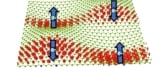
Undulations could replace twists in 2D materials
Though the transfer process is relatively smooth, Ago and colleagues acknowledge that it does produce some wrinkles and bubbles in the 2D materials. They are working on improvements to the composition of the adhesive layer that might help resolve this problem. Another focus for improvement is to increase the size of the transferred 2D materials beyond the 4-inch (102 mm) wafers they currently use.
“I also want to develop the fabrication of more sophisticated devices using different types of 2D materials and UV tapes,” Ago reveals. “These could substantially change the way electronic and photonics devices are produced.” Further collaborations with academia and industry, he says, could enable the team “to improve this unique tape transfer technique and push forward the realization of commercial products using 2D materials”.
- SEO Powered Content & PR Distribution. Get Amplified Today.
- PlatoData.Network Vertical Generative Ai. Empower Yourself. Access Here.
- PlatoAiStream. Web3 Intelligence. Knowledge Amplified. Access Here.
- PlatoESG. Carbon, CleanTech, Energy, Environment, Solar, Waste Management. Access Here.
- PlatoHealth. Biotech and Clinical Trials Intelligence. Access Here.
- Source: https://physicsworld.com/a/sticky-uv-sensitive-tape-makes-2d-material-transfers-easier/