By Külaline Autor postitatud 16
Global teams have mastered small-scale quantum computer design and are accelerating efforts to scale platforms with added qubits for enhanced computational power and quantum amplifiers for improved fidelity. Yet scaling up quantum systems escalates design complexity beyond the capabilities of typical quantum design workflows. These workflows, relying on separate point tools for tasks such as schematics, layout, electromagnetic simulation, and custom Python scripts for integration, present challenges for efficient management. Keysight QuantumPro arrives just in time, bringing an integrated workflow for the design of superconducting quantum computers.
Going where the photons go with a better yield
Why shouldn’t quantum design look more like cellular phone design? RF and digital disciplines have EDA tools to create chip, package, and board layouts, explore every part of a design, make data-based adjustments, and re-simulate from circuit to system level for optimization in one seamless workflow.
“Going where the photons go” for quantum computers (Figure 1) holds one crucial difference for quantum designers: step and replicate methods don’t finish the job. Successful quantum operations rely on precise design choices that create unique resonance frequencies within and between nearby qubits – overlapping two or more resonance frequencies leads to unpredictable cross-coupling results and a yield failure, often discovered the hard way at prototype cryogenic testing. Quantum designers must also worry about noise at cryogenic temperatures, kinetic inductance, non-linear quantum amplifier effects, and more.

Joonis 1. Comparing design, modeling, and analysis tasks between RF design and quantum design
Efficient system-level modeling and virtual design exploration are crucial to mitigate risks and costs associated with potential yield failures. Experienced quantum designers can create semi-automated workflows using various tools and scripts, which work smoothly when everything goes as planned. However, encountering issues leads to a cumbersome process of looping back, re-running scripts, adjusting formats, and potentially introducing errors, consuming valuable design time.
Automated quantum parameter extraction using various methods
QuantumPro integrates five functions (Figure 2) in a bundle built on Keysight Advanced Design System (ADS) for the seamless design of superconducting qubits and quantum amplifiers. Beginning with a schematic interface, users can effortlessly drag and drop components from the built-in quantum artworks. Layouts can be generated automatically from schematics, and then electromagnetic simulation is carried out in QuantumPro with automatic quantum parameter extraction.
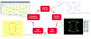
Joonis 2. Five functions seamlessly integrated into the QuantumPro workflow
Designers gain confidence in results with access to multiple electromagnetic solvers in QuantumPro. Full EM Analysis runs the finite element method (FEM) and the method of moments (MoM) solvers, sweeping frequency and producing S-parameters at input and output ports. The MoM solves only for currents on the metal surface instead of over a 3D volume, slashing computational costs. An Energy Participation Analysis allows for finding system eigenmodes using the FEM solver. Results from these analyses move into automated quantum parameter extraction with quasi-static, black box quantization, and energy participation ratio (EPR) methods.
QuantumPro users can see and compare quantum parameter extraction results in the same user interface where schematics and layouts exist, make necessary changes, and re-run extractions immediately. Users can also customize their workflow and user interface using Python scripts (Figure 3), making the leap from any previous semi-automated quantum workflow easier.
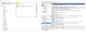
Joonis 3. Python scripting helps users customize the QuantumPro environment
Keeping pace with emerging quantum design technologies
Keysight developers are already at work on two recent arrivals in cutting-edge quantum design:
- Multi-layer quantum technology, scaling qubits by laying the chip out vertically in the same footprint,
- Josephson traveling-wave parametric amplifiers (JTWPAs), with elements arranged along a tight meandering path.
Both provide unique challenges with larger structures and more complex models. Multi-layer layouts are supported in QuantumPro and we have just released ADS2024U2 with new quantum artwork components that will assist designers in the layout of JTWPAs (Figure 4).
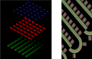
Joonis 4. Examples of multi-layer quantum technology (left) and a JTWPA layout (right) in ADS
Quantum computer scalability will ultimately hinge on design predictability. The seamless, automated quantum design workflow in QuantumPro makes it easier to focus efforts on creating optimized, predictable qubit and quantum amplifier designs instead of managing multiple EDA tools and conversions. Current and prospective quantum designers can learn more online:
Quantum EDA: ülijuhtivate kubittide kiiremad projekteerimistsüklid
- SEO-põhise sisu ja PR-levi. Võimenduge juba täna.
- PlatoData.Network Vertikaalne generatiivne Ai. Jõustage ennast. Juurdepääs siia.
- PlatoAiStream. Web3 luure. Täiustatud teadmised. Juurdepääs siia.
- PlatoESG. Süsinik, CleanTech, Energia, Keskkond päikeseenergia, Jäätmekäitluse. Juurdepääs siia.
- PlatoTervis. Biotehnoloogia ja kliiniliste uuringute luureandmed. Juurdepääs siia.
- Allikas: https://www.insidequantumtechnology.com/news-archive/automated-quantum-design-workflow-handles-higher-complexity-by-mohamed-hassan-keysight-technologies/